
Datasheet


Section 7 I/O Ports
Rev. 3.00 Sep. 28, 2009 Page 166 of 910
REJ09B0350-0300
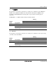
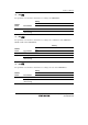
(7) P80/PME
The pin function is switched as shown below according to the combination of the register setting
of the LPC and the P80DDR bit.
Setting
LPC I/O Port
Module
Name
Pin Function
PME_OE P80DDR
LPC PME output
1 ⎯
I/O port P80 output 0 1
P80 input
(initial setting)
0 0
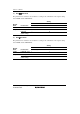
7.2.9 Port 9
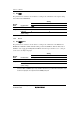
(1) P97/IRQ15/SDA0
The pin function is switched as shown below according to the combination of the IIC0AS and
IIC0BS bits in PTCNT1, ICE bit in ICCR of IIC_0, and the P97DDR bit. When the ISS15 bit in
ISSR16 is cleared to 0 and the IRQ15E bit in IER16 of the interrupt controller is set to 1, this pin
can be used as the IRQ15 input pin.
Setting
IIC_0 I/O Port
Module
Name
Pin Function
SDA0_OE P97DDR
IIC SDA0 input/output
1 ⎯
I/O port P97 output 0 1
P97 input
(initial setting)
0 0
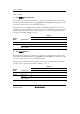
Note: To use this pin as SCL0, clear the IIC0AS and IIC0BS bits in PTCNT1 to 0. The output
format for SDA1 is NMOS output only and direct bus drive is possible. When this pin is used
as the P97 output pin, the output format is NMOS push-pull.