
Datasheet


Section 7 I/O Ports
Rev. 3.00 Sep. 28, 2009 Page 173 of 910
REJ09B0350-0300
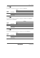
(3) PC5/WUE13/TIOCB1/TCLKC
The pin function is switched as shown below according to the combination of the register setting
of the TPU and the PC5DDR bit. When the WUEMR13 bit in WUEMR of the interrupt controller
is cleared to 0, this pin can be used as the WUE13 input pin.
This pin functions as TCLKC input when TPSC2 to TPSC0 in TCR_0 or TCR_2 is set to B'110 or
when channel 2 is set to phase counting mode.
This pin functions as TIOCB1 input when TPU channel 1 timer operating mode is set to normal
operation or phase counting mode and IOB3 to IOB0 in TIOR_1 are set to B'10xx. (x: Don't care.)
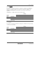
Setting
TPU I/O Port
Module
Name
Pin Function
TIOCB1_OE PC5DDR
TPU TIOCB1 output 1 ⎯
I/O port PC5 output 0 1
PC5 input
(initial setting)
0 0
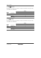
(4) PC4/WUE12/TIOCA1
The pin function is switched as shown below according to the combination of the register setting
of the TPU and the PC4DDR bit. When the WUEMR12 bit in WUEMR of the interrupt controller
is cleared to 0, this pin can be used as the WUE12 input pin.
This pin functions as TIOCA1 input when TPU channel 1 timer operating mode is set to normal
operation or phase counting mode and IOA3 to IOA0 in TIOR_1 are set to B'10xx. (x: Don't care.)
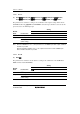
Setting
TPU I/O Port
Module
Name
Pin Function
TIOCA1_OE PC4DDR
TPU TIOCA1 output 1 ⎯
I/O port PC4 output 0 1
PC4 input
(initial setting)
0 0