
Datasheet


Section 7 I/O Ports
Rev. 3.00 Sep. 28, 2009 Page 178 of 910
REJ09B0350-0300
(2) PF3/TMOX/IRQ11/TDPCKI0/TDPMCI0
The pin function is switched as shown below according to the combination of the register setting
of the TMR and the PF3DDR bit. When the PMMS bit in TDPCR2_0 of TDP0 is set to 1, this pin
can be used as the TDPMCI0 input pin. When the external clock is selected by the CKS3 to CKS0
bits in TDPCR1_0 of TDP0, this pin is used as the TDPCKI0 input pin. Do not set input of
TDPCKI0 and TDPMCI0 at the same time. When the ISS11 bit in ISSR16 is cleared to 0 and the
IRQ11E bit in IER16 of the interrupt controller is set to 1, this pin can be used as the IRQ11 input
pin.
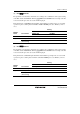
Setting
TMR I/O Port
Module
Name
Pin Function
TMOX_OE PF3DDR
TMR TMOX output 1 ⎯
I/O port PF3 output 0 1
PF3 input
(initial setting)
0 0
(3) PF2/TMOY/IRQ10/TDPCYI0
The pin function is switched as shown below according to the combination of the register setting
of the TMR and the PF2DDR bit. When the TDPIPE bit in TDPIER_0 of TDP0 is set to 1, this pin
can be used as the TDPCYI0 input pin. When the ISS10 bit in ISSR16 is cleared to 0 and the
IRQ10E bit in IER16 of the interrupt controller is set to 1, this pin can be used as the IRQ10 input
pin.
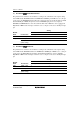
Setting
TMR I/O Port
Module
Name
Pin Function
TMOY_OE PF2DDR
TMR TMOY output 1 ⎯
I/O port PF2 output 0 1
PF2 input
(initial setting)
0 0