
Datasheet


Section 10 16-Bit Timer Pulse Unit (TPU)
Rev. 3.00 Sep. 28, 2009 Page 248 of 910
REJ09B0350-0300
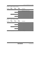
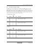
Table 10.9 MD3 to MD0
Bit 3
MD3*
1
Bit2
MD2*
2
Bit 1
MD1
Bit 0
MD0
Description
0 Normal operation
0
1 Reserved
0 PWM mode 1
0
1
1 PWM mode 2
0 Phase counting mode 1 0
1 Phase counting mode 2
0 Phase counting mode 3
0
1
1
1 Phase counting mode 4
1 × × × Setting prohibited
[Legend]
x: Don't care
Notes: 1. MD3 is reserved bit. In a write, it should be written with 0.
2. Phase counting mode cannot be set for channels 0 and 3. In this case, 0 should always
be written to MD2.