
Datasheet

Section 15 Serial Communication Interface (SCI)
Rev. 3.00 Sep. 28, 2009 Page 408 of 910
REJ09B0350-0300
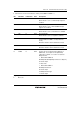
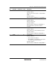
Bit Bit Name Initial Value R/W Description
4 O/E 0 R/W Parity Mode (valid only when the PE bit is 1 in
asynchronous mode)
0: Selects even parity
1: Selects odd parity
For details on the usage of this bit in smart card
interface mode, see section 15.7.2, Data Format
(Except in Block Transfer Mode).
3
2
BCP1
BCP0
0
0
R/W
R/W
Basic Clock Pulse 1 and 0
These bits select the number of basic clock cycles in
a 1-bit data transfer time in smart card interface
mode.
00: 32 clock cycles (S = 32)
01: 64 clock cycles (S = 64)
10: 372 clock cycles (S = 372)
11: 256 clock cycles (S = 256)
For details, see section 15.7.4, Receive Data
Sampling Timing and Reception Margin. S is
described in section 15.3.9, Bit Rate Register
(BRR).
1
0
CKS1
CKS0
0
0
R/W
R/W
Clock Select 1 and 0
These bits select the clock source for the baud rate
generator.
00: φ clock (n = 0)
01: φ/4 clock (n = 1)
10: φ/16 clock (n = 2)
11: φ/64 clock (n = 3)
For the relation between the bit rate register setting
and the baud rate, see section 15.3.9, Bit Rate
Register (BRR). n is the decimal display of the value
of n in BRR (see section 15.3.9, Bit Rate Register
(BRR)).
Note: * etu: Element Time Unit (time taken to transfer one bit)