
Datasheet


Section 15 Serial Communication Interface (SCI)
Rev. 3.00 Sep. 28, 2009 Page 443 of 910
REJ09B0350-0300
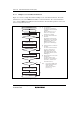
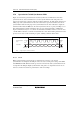
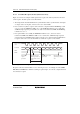
Transfer direction
Bit 0
Serial data
Synchronization
clock
1 frame
TDRE
TEND
Data written to TDR and
TDRE flag cleared to 0 in
TXI interrupt service
routine
TXI interrupt request
generated
Bit 1 Bit 7 Bit 0 Bit 1 Bit 6 Bit 7
TXI interrupt request
generated
TEI interrupt request
generated
Figure 15.16 Sample SCI Transmission Operation in Clocked Synchronous Mode
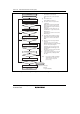
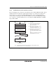
No
[1]
Yes
Initialization
Start transmission
Read TDRE flag in SSR
[2]
Write transmit data to TDR and
clear TDRE flag in SSR to 0
No
Yes
No
Yes
Read TEND flag in SSR
[3]
Clear TE bit in SCR to 0
TDRE = 1
All data transmitted?
TEND = 1
[1] SCI initialization:
The TxD pin is automatically
designated as the transmit data
output pin.
[2] SCI status check and transmit data
write:
Read SSR and check that the TDRE
flag is set to 1, then write transmit
data to TDR and clear the TDRE flag
to 0.
[3] Serial transmission continuation
procedure:
To continue serial transmission, be
sure to read 1 from the TDRE flag to
confirm that writing is possible, then
write data to TDR, and then clear the
TDRE flag to 0.
Note: Do not write to SMR, SCR,
BRR, and SDCR from the
start to the end of
transmission except the
process of [4].
[4]
End transmission
Figure 15.17 Sample Serial Transmission Flowchart