
Datasheet

Section 18 Keyboard Buffer Control Unit (PS2)
Rev. 3.00 Sep. 28, 2009 Page 579 of 910
REJ09B0350-0300
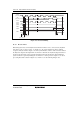
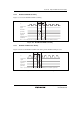
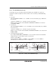
18.4.4 KCLKI and KDI Read Timing
Figure 18.9 shows the KCLKI and KDI read timing.
T1 T2
φ*
Internal read
signal
Note: * φ here indicates the clock signal frequency-divided by N for medium-speed mode.
KCLK, KD
(pin state)
KCLKI, KDI
(register)
Internal data bus
(read data)
Figure 18.9 KCLKI and KDI Read Timing
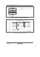
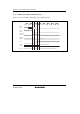
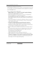
18.4.5 KCLKO and KDO Write Timing
Figure 18.10 shows the KLCKO and KDO write timing and the KCLK and KD pin states.
Internal write
signal
KCLKO, KDO
(register)
KCLK, KD
(pin state)
T1 T2
φ*
Note: * φ here indicates the clock signal frequency-divided by N for medium-speed mode.
Figure 18.10 KCLKO and KDO Write Timing