
Datasheet


Section 20 A/D Converter
Rev. 3.00 Sep. 28, 2009 Page 671 of 910
REJ09B0350-0300
20.7.6 Notes on Noise Countermeasures
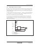
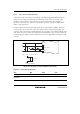
A protection circuit connected to prevent damage of the analog input pins (AN0 to AN15) and
analog reference voltage pin (AVref) due to an abnormal voltage such as an excessive surge
should be connected between AVcc and AVss, as shown in figure 20.6. Also, the bypass
capacitors connected to AVcc and AVref, and the filter capacitors connected to AN0 to AN15
must be connected to AVss.
If a filter capacitor is connected, the input currents at the analog input pins (AN0 to AN15) are
averaged, and so an error may arise. Also, when A/D conversion is performed frequently, as in
scan mode, if the current charged and discharged by the capacitance of the sample-and-hold circuit
in the A/D converter exceeds the current input via the input impedance (R
in
), an error will arise in
the analog input pin voltage. Careful consideration is therefore required when deciding the circuit
constants.
AV
CC
*
1
*
1
AN0 to AN15
AV
SS
Notes: Values are reference values.
1.
2. R
in
: Input impedance
R
in
*
2
100 Ω
0.1 µF
0.01 µF10 µF
AV
ref
Figure 20.6 Example of Analog Input Protection Circuit
Table 20.7 Analog Pin Specifications
Item Min. Max. Unit
Analog input capacitance ⎯ 20 pF
Permissible signal-source
impedance
⎯ 5 kΩ