
Datasheet


Section 22 Flash Memory
Rev. 3.00 Sep. 28, 2009 Page 709 of 910
REJ09B0350-0300
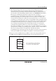
The procedure program must be executed in an area other than the flash memory to be
programmed. Setting the SCO bit in FCCS to 1 to request download must be executed in the on-
chip RAM. The area that can be executed in the steps of the procedure program (on-chip RAM,
user MAT, and external space) is shown in section 22.8.4, Storable Areas for On-Chip Program
and Program Data. The following description assumes that the area to be programmed on the user
MAT is erased and that program data is prepared in the consecutive area.
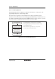
The program data for one programming operation is always 128 bytes. When the program data
exceeds 128 bytes, the start address of the programming destination and program data parameters
are updated in 128-byte units and programming is repeated. When the program data is less than
128 bytes, invalid data is filled to prepare 128-byte program data. If the invalid data to be added is
H'FF, the program processing time can be shortened.
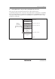
1. Select the on-chip program to be downloaded and the download destination. When the PPVS
bit in FPCS is set to 1, the programming program is selected. Several programming/erasing
programs cannot be selected at one time. If several programs are selected, a download error is
returned to the SS bit in the DPFR parameter. The on-chip RAM start address of the download
destination is specified by FTDAR.
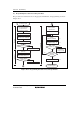
2. Write H'A5 in FKEY. If H'A5 is not written to FKEY, the SCO bit in FCCS cannot be set to 1
to request download of the on-chip program.
⎯ H'A5 is written to FKEY.
⎯ Setting the SCO bit is executed in the on-chip RAM.
When the SCO bit is set to 1, download is started automatically. Since the SCO bit is cleared
to 0 when the procedure program is resumed, the SCO bit cannot be confirmed to be 1 in the
procedure program. The download result can be confirmed by the return value of the DPFR
parameter. To prevent incorrect decision, before setting the SCO bit to 1, set one byte of the
on-chip RAM start address specified by FTDAR, which becomes the DPFR parameter, to a
value other than the return value (e.g. H'FF). Particular processing that is accompanied by bank
switching as described below is performed when download is executed. Dummy read of FCCS
must be performed twice immediately after the SCO bit is set to 1.
⎯ The user-MAT space is switched to the on-chip program storage area.
⎯ After the program to be downloaded and the on-chip RAM start address specified by
FTDAR are checked, they are transferred to the on-chip RAM.
⎯ FPCS, FECS, and the SCO bit in FCCS are cleared to 0.
⎯ The return value is set in the DPFR parameter.
⎯ The values of general registers of the CPU are held.
⎯ During download, no interrupts can be accepted. However, since the interrupt requests are
held, when the procedure program is resumed, the interrupts are requested.