
Datasheet


Section 23 Clock Pulse Generator
Rev. 3.00 Sep. 28, 2009 Page 759 of 910
REJ09B0350-0300
Section 23 Clock Pulse Generator
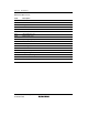
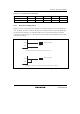
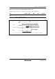
This LSI incorporates a clock pulse generator which generates the system clock (φ), internal clock,
bus master clock, and subclock (φSUB). The clock pulse generator consists of an oscillator, duty
correction circuit, system clock select circuit, subclock input circuit, and subclock waveform
forming circuit. Figure 23.1 shows a block diagram of the clock pulse generator.
EXTAL
XTAL
EXCL
(ExEXCL)
WDT_1
count clock
φ
φSUB
Subclock
input circuit
Subclock
waveform
forming circuit
Oscillator
System clock
to
φ
pin
Internal clock
to on-chip
peripheral modules
System
clock
select
circuit
Bus master
clock to CPU
φ
Duty
correction
circuit
Figure 23.1 Block Diagram of Clock Pulse Generator
The subclock input is controlled by software according to the EXCLE bit and the EXCLS bit in
the port control register (PTCNT0) settings in the low power control register (LPWRCR). For
details on LPWRCR, see section 24.1.2, Low-Power Control Register (LPWRCR). For details on
PTCNT0, see section 7.3.1, Port Control Register 0 (PTCNT0).