
Datasheet


Section 23 Clock Pulse Generator
Rev. 3.00 Sep. 28, 2009 Page 764 of 910
REJ09B0350-0300
23.2 Duty Correction Circuit
The duty correction circuit generates the system clock (φ) by correcting the duty of the clock
output from the oscillator.
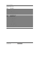
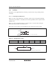
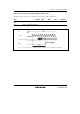
23.3 Subclock Input Circuit
The subclock input circuit controls subclock input from the EXCL or ExEXCL pin. To use the
subclock, a 32.768-kHz external clock should be input from the EXCL or ExEXCL pin.
Figure 23.7 shows the relationship of subclock input from the EXCL pin and the ExEXCL pin.
When using a pin to input the subclock, specify input for the pin by clearing the DDR bit of the
pin to 0. The EXCL pin is specified as an input pin by clearing the EXCLS bit in PTCNT0 to 0.
The ExEXCL pin is specified as an input pin by setting the EXCLS bit in PTCNT0 to 1. The
subclock input is enabled by setting the EXCLE bit in LPWRCR to 1.
P96/EXCL
EXCLS
(PTCNT0)
EXCLE
(LPWRCR)
PE0/ExEXCL
Subcloc
k
Figure 23.7 Subclock Input from EXCL Pin and ExEXCL Pin
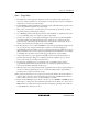
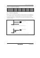
Subclock input conditions are shown in table 23.5. When the subclock is not used, subclock input
should not be enabled.
Table 23.5 Subclock Input Conditions
VCC = 3.0 to 3.6 V
Item Symbol Min. Typ. Max. Unit Test Conditions
Subclock input pulse width
low level
t
EXCLL
⎯ 15.26 ⎯ μs
Subclock input pulse width
high level
t
EXCLH
⎯ 15.26 ⎯ μs
Subclock input rising time t
EXCLr
⎯ ⎯ 10 ns
Figure 23.8
Subclock input falling time t
EXCLf
⎯ ⎯ 10 ns