
Datasheet


Section 26 Electrical Characteristics
Rev. 3.00 Sep. 28, 2009 Page 875 of 910
REJ09B0350-0300
Section 26 Electrical Characteristics
26.1 Absolute Maximum Ratings
Table 26.1 lists the absolute maximum ratings.
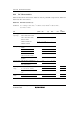
Table 26.1 Absolute Maximum Ratings
Item Symbol Value Unit
Power supply voltage* V
CC
–0.3 to +4.3
Input voltage (except ports 7, D, A, G, I, PE4,
PE2 to PE0, P97, P86, P52, and P42)
V
in
–0.3 to V
CC
+ 0.3
Input voltage (ports A, G, I, PE4, PE2 to PE0,
P97, P86, P52, and P42)
V
in
–0.3 to +7.0
Input voltage (AN input is not selected for port
D)
V
in
–0.3 to V
CC
+ 0.3
Input voltage (AN input is selected for port D) V
in
–0.3 to V
CC
+0.3 or –0.3 to AV
CC
+0.3 whichever is lower
Input voltage (port 7) V
in
–0.3 to AV
CC
+ 0.3
Reference power supply voltage AVref –0.3 to AV
CC
+ 0.3
Analog power supply voltage AV
CC
–0.3 to +4.3
Analog input voltage V
AN
–0.3 to AV
CC
+ 0.3
V
Operating temperature T
opr
–20 to +75
Operating temperature (when flash memory is
programmed or erased)
T
opr
0 to +75
°C
Storage temperature T
stg
–55 to +125
Caution: Permanent damage to this LSI may result if absolute maximum ratings are exceeded.
Make sure the applied power supply does not exceed 4.3 V.
Note: * Voltage applied to the VCC pin.
The VCL pin should not be applied a voltage.