
Datasheet


Section 9 8-Bit PWM Timer (PWM)
Rev. 3.00 Mar 21, 2006 page 236 of 788
REJ09B0300-0300
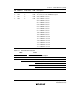
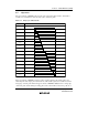
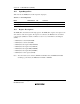
Table 9.3 Resolution, PWM Conversion Period and Carrier Frequency when φ
φφ
φ = 10 MHz
Internal Clock
Frequency
Resolution
PWM Conversion
Period
Carrier Frequency
φ 100 ns 25.6 µs 625 kHz
φ/2 200 ns 51.2 µs 312.5 kHz
φ/4 400 ns 102.4 µs 156.3 kHz
φ/8 800 ns 204.8 µs 78.1 kHz
φ/16 1600 ns 409.6 µs 39.1 kHz
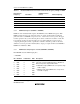
9.3.2 PWM Data Registers (PWDR0 to PWDR15)
PWDR are 8-bit readable/writable registers. The PWM has sixteen PWM data registers. Each
PWDR specifies the duty cycle of the basic pulse to be output, and the number of additional
pulses. The value set in PWDR corresponds to a 0 or 1 ratio in the conversion period. The upper
four bits specify the duty cycle of the basic pulse as 0/16 to 15/16 with a resolution of 1/16. The
lower four bits specify how many extra pulses are to be added within the conversion period
comprising 16 basic pulses. Thus, a specification of 0/256 to 255/256 is possible for 0/1 ratios
within the conversion period. For 256/256 (100%) output, port output should be used. PWDR0 to
PWDR15 are initialized to H'00.
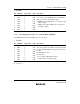
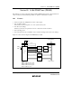
9.3.3 PWM Data Polarity Registers A and B (PWDPRA, PWDPRB)
Each PWDPR selects the PWM output phase.
• PWDPRA
Bit Bit Name Initial Value R/W Description
7
6
5
4
3
2
1
0
OS7
OS6
OS5
OS4
OS3
OS2
OS1
OS0
0
0
0
0
0
0
0
0
R/W
R/W
R/W
R/W
R/W
R/W
R/W
R/W
Output Select 7 to 0
These bits select the PWM output phase. Bits OS7 to
OS0 correspond to outputs PW7 to PW0.
0: PWM direct output (PWDR value corresponds to high
width of output)
1: PWM inverted output (PWDR value corresponds to
low width of output)