
Datasheet

Section 23 ROM
Rev. 3.00 Mar 21, 2006 page 618 of 788
REJ09B0300-0300
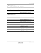
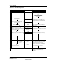
Table 23.4 On-Board Programming Mode Settings
Mode Setting MD1 MD0 P92 P91 P90
Boot mode 0 0 1
*
1
*
1
*
Mode 2 (advanced mode) 1 0 User program
mode
Mode 3 (normal mode) 1 1
Note: * Can be used as an I/O port after the boot mode activation.
23.7.1 Boot Mode
Table 23.5 shows the boot mode operations between reset end and branching to the programming
control program.
1. When boot mode is used, the flash memory programming control program must be prepared in
the host beforehand. Prepare a programming control program in accordance with the
description in section 23.8, Flash Memory Programming/Erasing. In boot mode, if any data
exists in the flash memory (except in the case that all data are 1), all blocks in the flash
memory are erased. Use boot mode at initial writing in the on-board state, or forced recovery
when user program mode cannot be executed because the program to be initiated in user
program mode was mistakenly erased.
2. The SCI_1 should be set to asynchronous mode, and the transfer format as follows: 8-bit data,
1 stop bit, and no parity.
3. When the boot program is initiated, this LSI measures the low-level period of asynchronous
SCI communication data (H'00) transmitted continuously from the host. This LSI then
calculates the bit rate of transmission from the host, and adjusts the SCI_1 bit rate to match
that of the host. The reset should end with the RxD1 pin high. The RxD1 and TxD1 pins
should be pulled up on the board if necessary. After the reset ends, it takes approximately 100
states before this LSI is ready to measure the low-level period.
4. After matching the bit rates, this LSI transmits one H'00 byte to the host to indicate the end of
bit rate adjustment. The host should confirm that this adjustment end indication (H'00) has
been received normally, and transmit one H'55 byte to this LSI. If reception could not be
performed normally, initiate boot mode again by a reset. Depending on the host’s transfer bit
rate and system clock frequency of this LSI, there will be a discrepancy between the bit rates
of the host and this LSI. To operate the SCI properly, set the host’s transfer bit rate and system
clock frequency of this LSI within the ranges listed in table 23.6.
5. In boot mode, a part of the on-chip RAM area is used by the boot program. Addresses
H'FFE080 to H'FFE87F
*
1
is the area to which the programming control program is transferred
from the host. Note, however, that ID codes are assigned to addresses H'FFE080 to
H'FFE087
*
2
. The boot program area cannot be used until the execution state in boot mode