
Datasheet


Section 27 Electrical Characteristics
Rev. 3.00 Mar 21, 2006 page 728 of 788
REJ09B0300-0300
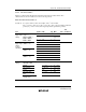
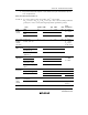
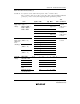
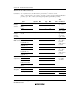
Item Symbol Min Typ Max Unit
Test
Conditions
RES, STBY,
MD1, MD0
–0.3 — 0.5
PA7 to PA0
(3)
–0.3 — 1.0
Input low
voltage
NMI, EXTAL,
input pins except (1)
and (3) above
V
IL
–0.3 — 0.8
V
V
CC
– 0.5
V
CC
B – 0.5
—— VI
OH
= –200 µAAll output pins
(except P97, P86,
P52, and P42)
*
5
*
8
3.5 —— VI
OH
= –1 mA,
Output high
voltage
P97, P86, P52, and
P42
*
4
V
OH
2.0 —— VI
OH
= –200 µA
All output pins
(except RESO)
*
5
——0.4 V I
OL
= 1.6 mA
Ports 1 to 3 ——1.0 V I
OL
= 10 mA
Output low
voltage
RESO
V
OL
——0.4 V I
OL
= 2.6 mA
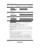
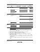
Notes: 1. Do not leave the AV
CC
, AV
ref
, and AV
SS
pins open even if the A/D converter and D/A
converter are not used.
Even if the A/D converter and D/A converter are not used, apply a value in the range
2.0 V to 5.5 V to AV
CC
and AV
ref
pins by connection to the power supply (V
CC
), or some
other method. Ensure that AV
ref
≤ AV
CC
.
2. P67 to P60 include peripheral module inputs multiplexed on those pins.
3. IRQ2 includes the ADTRG signal multiplexed on that pin.
4. P52/SCK0/SCL0, P97/SDA0, P86/SCK1/SCL1, P42/SCK2/SDA1, and port G are
NMOS push-pull outputs.
When the SCL0, SDA0, SCL1, or SDA1 (ICE = 1) pin is used as an output, it is NMOS
open-drain output. Therefore, an external pull-up resistor must be connected in order to
output high level.
P52/SCK0, P97, P86/SCK1, P42/SCK2 (ICE = 0), and port G high levels are driven by
NMOS.
When the SCK0, SCK1, or SCK2 pin is used as an output, an external pull-up resistor
must be connected in order to output high level.
5. When IICS = 0, ICE = 0, and KBIOE = 0. Low-level output when the bus drive function
is selected is determined separately.
6. The upper limit of the port 6 applied voltage is V
CC
+ 0.3 V when CIN input is not
selected, and the lower of V
CC
+ 0.3 V and AV
CC
+ 0.3 V when CIN input is selected.
When a pin is in output mode, the output voltage is equivalent to the applied voltage.
7. The upper limit of the port A applied voltage is V
CC
B + 0.3 V when CIN input is not
selected, and the lower of V
CC
B + 0.3 V and AV
CC
+ 0.3 V when CIN input is selected.
When a pin is in output mode, the output voltage is equivalent to the applied voltage.