
Datasheet


Appendix B Internal I/O Registers
Rev. 4.00 Sep 27, 2006 page 1083 of 1130
REJ09B0327-0400
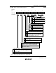
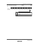
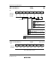
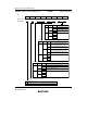
TCONRO—Timer Connection Register O H'FFFD Timer Connection
Bit
Initial value
Read/Write
7
HOE
0
R/W
6
VOE
0
R/W
5
CLOE
0
R/W
4
CBOE
0
R/W
3
HOINV
0
R/W
0
CBOINV
0
R/W
2
VOINV
0
R/W
1
CLOINV
0
R/W
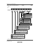
Output synchronization
signal inversion
0
The CBLANK signal is
used directly as the
CBLANK output
1 The CBLANK signal is
inverted before use as
the CBLANK output
Output synchronization signal inversion
0
The CLO signal (CL1, CL2, CL3,
or CL4 signal) is used directly as
the CLAMPO output
1 The CLO signal (CL1, CL2, CL3,
or CL4 signal) is inverted before
use as the CLAMPO output
Output synchronization signal inversion
0
The IVO signal is used directly as
the VSYNCO output
1 The IVO signal is inverted before
use as the VSYNCO output
Output synchronization signal inversion
0
The IHO signal is used directly as the HSYNCO output
1 The IHO signal is inverted before use as the HSYNCO output
Output enable
0
The P27/A15/PW15/CBLANK pin functions as the P27/A15/PW15 pin
1 In mode 1 (expanded mode with on-chip ROM disabled):
The P27/A15/PW15/CBLANK pin functions as the A15 pin
In modes 2 and 3 (expanded modes with on-chip ROM enabled):
The P27/A15/PW15/CBLANK pin functions as the CBLANK pin
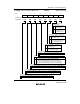
Output enable
0
The P64/FTIC/KIN4/CIN4/CLAMPO pin functions as the P64/FTIC/KIN4/CIN4 pin
1 The P64/FTIC/KIN4/CIN4/CLAMPO pin functions as the CLAMPO pin
Output enable
0
The P61/FTOA/KIN1/CIN1/VSYNCO pin functions as the P61/FTOA/KIN1/CIN1 pin
1 The P61/FTOA/KIN1/CIN1/VSYNCO pin functions as the VSYNCO pin
Output enable
0
The P44/TMO1/HIRQ1/HSYNCO pin functions as the P44/TMO1/HIRQ1 pin
1 The P44/TMO1/HIRQ1/HSYNCO pin functions as the HSYNCO pin