
Datasheet


Appendix C I/O Port Block Diagrams
Rev. 4.00 Sep 27, 2006 page 1104 of 1130
REJ09B0327-0400
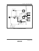
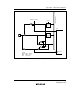
R
QD
D
KMPCR
C
Reset
R
QD
P66DR
C
Reset
WP6P
R
Q
P66DDR
C
Reset
WP6D
WP6
16-bit FRT
FTOB output
Output enable
A/D converter
Analog input
IRQ6 input
KMIMR6
Other
key-sense interrupt inputs
IRQ6 enable
P66
RP6P
RP6
WP6P: Write to P6PCR
WP6D: Write to P6DDR
WP6: Write to port 6
RP6P: Read P6PCR
RP6: Read port 6
Hardware
standby
Internal data bus
Legend:
Figure C.19 Port 6 Block Diagram (Pin P66)