
Datasheet

Appendix C I/O Port Block Diagrams
Rev. 4.00 Sep 27, 2006 page 1111 of 1130
REJ09B0327-0400
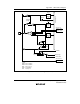
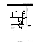
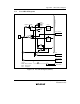
D
R
QD
P85DR
C
Reset
R
Q
P85DDR
C
Reset
Hardware standby
WP8D
WP8
SCI1
Input enable
Serial receive data
IRQ4 input
IRQ4 enable
P85
RP8
WP8D: Write to P8DDR
WP8: Write to port 8
RP8: Read port 8
Internal data bus
Legend:
Figure C.27 Port 8 Block Diagram (Pin P85)