
Datasheet

Section 8 I/O Ports
Rev. 4.00 Sep 27, 2006 page 231 of 1130
REJ09B0327-0400
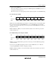
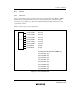
A15 (Output)/P27 (Output)
A14 (Output)/P26 (Output)
A13 (Output)/P25 (Output)
A12 (Output)/P24 (Output)
A11 (Output)
A10 (Output)
A9 (Output)
A8 (Output)
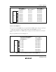
Port 2
When P2DDR = 1
and PWOERB = 0
P27 (Input)/CBLANK (Output)
P26 (Input)
P25 (Input)
P24 (Input)
P23 (Input)
P22 (Input)
P21 (Input)
P20 (Input)
When P2DDR = 0
PW15 (Output)/CBLANK (Output)
PW14 (Output)
PW13 (Output)
PW12 (Output)
PW11 (Output)
PW10 (Output)
PW9 (Output)
PW8 (Output)
When P2DDR = 1
and PWOERB = 1
Figure 8.7 Port 2 Pin Functions (Modes 2 and 3 (EXPE = 1))
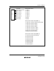
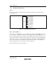
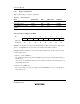
Modes 2 and 3 (EXPE = 0)
In modes 2 and 3 (when EXPE = 0), port 2 pins function as PWM outputs (P27 can also function
as the timer connection output (CBLANK)) or I/O ports, and input or output can be specified on a
bit-by-bit basis. When a bit in P2DDR is set to 1, the corresponding pin functions as a PWM
output or output port, and when cleared to 0, as an input port. P27 can be used as an on-chip
supporting module output pin regardless of the P27DDR setting.
The port 2 pin functions are shown in figure 8.8.
P27 (I/O)/CBLANK (Output)
P26 (I/O)
P25 (I/O)
P24 (I/O)
P23 (I/O)
P22 (I/O)
P21 (I/O)
P20 (I/O)
Port 2
P2n: Input pin when P2DDR = 0,
output pin when P2DDR = 1
and PWOERB = 0
PW15 (Output)/CBLANK (Output)
PW14 (Output)
PW13 (Output)
PW12 (Output)
PW11 (Output)
PW10 (Output)
PW9 (Output)
PW8 (Output)
When P2DDR = 1
and PWOERB = 1
Figure 8.8 Port 2 Pin Functions (Modes 2 and 3 (EXPE = 0))