
Datasheet


Section 15 Serial Communication Interface (SCI, IrDA)
Rev. 4.00 Sep 27, 2006 page 450 of 1130
REJ09B0327-0400
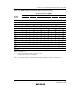
Bit 2—Data Invert (SINV): Specifies inversion of the data logic level. The SINV bit does not
affect the logic level of the parity bit(s): parity bit inversion requires inversion of the O/E bit in
SMR.
Bit 2
SINV Description
0 TDR contents are transmitted without modification (Initial value
)
Receive data is stored in RDR without modification
1 TDR contents are inverted before being transmitted
Receive data is stored in RDR in inverted form
Bit 1—Reserved: This bit cannot be modified and is always read as 1.
Bit 0—Serial Communication Interface Mode Select (SMIF): Reserved bit. 1 should not be
written in this bit.
Bit 0
SMIF Description
0 Normal SCI mode (Initial value
)
1 Reserved mode
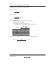
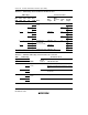
15.2.10 Module Stop Control Register (MSTPCR)
7
MSTP15
0
R/W
Bit
Initial value
Read/Write
6
MSTP14
0
R/W
5
MSTP13
1
R/W
4
MSTP12
1
R/W
3
MSTP11
1
R/W
2
MSTP10
1
R/W
1
MSTP9
1
R/W
0
MSTP8
1
R/W
7
MSTP7
1
R/W
6
MSTP6
1
R/W
5
MSTP5
1
R/W
4
MSTP4
1
R/W
3
MSTP3
1
R/W
2
MSTP2
1
R/W
1
MSTP1
1
R/W
0
MSTP0
1
R/W
MSTPCRH MSTPCRL
MSTPCR, comprising two 8-bit readable/writable registers, performs module stop mode control.
When bit MSTP7, MSTP6, or MSTP5 is set to 1, SCI0, SCI1, or SCI2 operation, respectively,
stops at the end of the bus cycle and a transition is made to module stop mode. For details, see
section 25.5, Module Stop Mode.
MSTPCR is initialized to H'3FFF by a reset and in hardware standby mode. It is not initialized in
software standby mode.