
Datasheet


Section 22 ROM (Mask ROM Version, H8S/2148 F-ZTAT, H8S/2147N F-ZTAT, H8S/2144 F-ZTAT, and H8S/2142 F-ZTAT)
Rev. 4.00 Sep 27, 2006 page 653 of 1130
REJ09B0327-0400
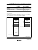
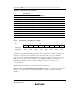
22.5.3 Erase Block Registers 1 and 2 (EBR1, EBR2)
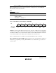
Bit 76543210
EBR1 ——————EB9/—
*
2
EB8/—
*
2
Initial value00000000
Read/Write ——————R/W
*
1
*
2
R/W
*
1
*
2
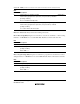
Bit 76543210
EBR2 EB7 EB6 EB5 EB4 EB3 EB2 EB1 EB0
Initial value00000000
Read/Write R/W
*
1
R/W R/W R/W R/W R/W R/W R/W
Notes: 1. In normal mode, these bits cannot be modified and are always read as 0.
2. Bits EB8 and EB9 are not present in the 64-kbyte versions; they must not be set to 1.
EBR1 and EBR2 are registers that specify the flash memory erase area block by block; bits 1 and
2 in EBR1 (128 kB versions only) and bits 7 to 0 in EBR2 are readable/writable bits. EBR1 and
EBR2 are each initialized to H'00 by a reset, in hardware standby mode, software standby mode,
subactive mode, subsleep mode, and watch mode, and the SWE bit in FLMCR1 is not set. When a
bit in EBR1 or EBR2 is set, the corresponding block can be erased. Other blocks are erase-
protected. Set only one bit in EBR1 or EBR2 (more than one bit cannot be set). When on-chip
flash memory is disabled, a read will return H'00, and writes are invalid.
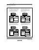
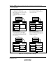
The flash memory block configuration is shown in table 22.5.