
Datasheet


Section 2 CPU
Rev. 4.00 Sep 27, 2006 page 80 of 1130
REJ09B0327-0400
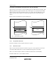
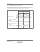
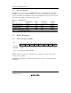
2.9.3 On-Chip Supporting Module Access Timing
The on-chip supporting modules are accessed in two states. The data bus is either 8 bits or 16 bits
wide, depending on the particular internal I/O register being accessed. Figure 2.19 shows the
access timing for the on-chip supporting modules. Figure 2.20 shows the pin states.
Bus cycle
T1 T2
Address
Read data
Write data
Internal read signal
Internal data bus
Internal write signal
Internal data bus
Read
access
Write
access
Internal address bus
φ
Figure 2.19 On-Chip Supporting Module Access Cycle