
Datasheet


Section 2 CPU
Rev. 4.00 Sep 27, 2006 page 81 of 1130
REJ09B0327-0400
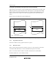
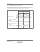
Bus cycle
T1 T2
Unchanged
Address bus
AS
RD
HWR, LWR
Data bus
φ
High
High
High
High impedance
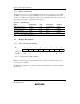
Figure 2.20 Pin States during On-Chip Supporting Module Access
2.9.4 External Address Space Access Timing
The external address space is accessed with an 8-bit or 16-bit data bus width in a two-state or
three-state bus cycle. In three-state access, wait states can be inserted. For further details, refer to
section 6, Bus Controller.