
Datasheet

Section 5 Interrupt Controller
Rev. 4.00 Sep 27, 2006 page 145 of 1130
REJ09B0327-0400
5.5.5 Interrupt Response Times
This LSI are capable of fast word access to on-chip memory, and high-speed processing can be
achieved by providing the program area in on-chip ROM and the stack area in on-chip RAM.
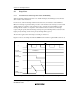
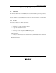
Table 5.8 shows interrupt response times—the interval between generation of an interrupt request
and execution of the first instruction in the interrupt handling routine. The symbols used in table
5.8 are explained in table 5.9.
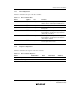
Table 5.8 Interrupt Response Times
Number of States
No. Item Normal Mode Advanced Mode
1 Interrupt priority determination
*
1
33
2 Number of wait states until executing
instruction ends
*
2
1 to 19+2·S
I
1 to 19+2·S
I
3 PC, CCR stack save 2·S
K
2·S
K
4 Vector fetch S
I
2·S
I
5 Instruction fetch
*
3
2·S
I
2·S
I
6 Internal processing
*
4
22
Total (using on-chip memory) 11 to 31 12 to 32
Notes: 1. Two states in case of internal interrupt.
2. Refers to MULXS and DIVXS instructions.
3. Prefetch after interrupt acceptance and interrupt handling routine prefetch.
4. Internal processing after interrupt acceptance and internal processing after vector fetch.
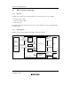
Table 5.9 Number of States in Interrupt Handling Routine Execution
Object of Access
External Device
8-Bit Bus 16-Bit Bus
Symbol
Internal
Memory
2-State
Access
3-State
Access
2-State
Access
3-State
Access
Instruction fetch S
I
1 4 6+2m 2 3+m
Branch address read S
J
Stack manipulation S
K
Legend:
m: Number of wait states in an external device access