
Datasheet

Section 8 I/O Ports
Rev. 4.00 Sep 27, 2006 page 242 of 1130
REJ09B0327-0400
Pin Selection Method and Pin Functions
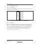
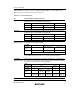
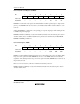
P41/TMO0/RxD2/
IrRxD
The pin function is switched as shown below according to the combination of
bits OS3 to OS0 in TCSR of TMR0, bit RE in SCR of SCI2 and bit P41DDR.
OS3 to OS0 All 0 Not all 0
RE 0 1 0
P41DDR 0 1 ——
Pin function P41
input pin
P41
output pin
RxD2/IrRxD
input pin
TMO0
output pin
When this pin is used as the TMO0 output pin, bit RE in SCR of SCI2 must be
cleared to 0.
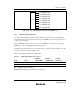
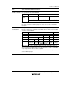
P40/TMCI0/TxD2/
IrTxD
The pin function is switched as shown below according to the combination of
bit TE in SCR of SCI2 and bit P40DDR.
TE 0 1
P40DDR 0 1 —
Pin function P40
input pin
P40
output pin
TxD2/IrTxD
output pin
TMCI0 input pin
When an external clock is selected with bits CKS2 to CKS0 in TCR0 of TMR0,
this pin is used as the TMCI0 input pin.