
Datasheet

Section 8 I/O Ports
Rev. 4.00 Sep 27, 2006 page 260 of 1130
REJ09B0327-0400
8.10.2 Register Configuration
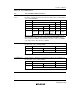
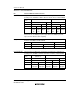
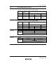
Table 8.20 summarizes the port 9 registers.
Table 8.20 Port 9 Registers
Name Abbreviation R/W Initial Value Address
*
1
Port 9 data direction register P9DDR W H'40/H'00
*
2
H'FFC0
Port 9 data register P9DR R/W H'00 H'FFC1
Notes: 1. Lower 16 bits of the address.
2. Initial value depends on the mode.
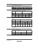
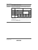
Port 9 Data Direction Register (P9DDR)
Bit 76543210
P97DDR P96DDR P95DDR P94DDR P93DDR P92DDR P91DDR P90DDR
Mode 1
Initial value01000000
Read/Write W W W W W W W W
Modes 2 and 3
Initial value00000000
Read/Write W W W W W W W W
P9DDR is an 8-bit write-only register, the individual bits of which specify input or output for the
pins of port 9. P9DDR cannot be read; if it is, an undefined value will be returned.
P9DDR is initialized to H'40 (mode 1) or H'00 (modes 2 and 3) by a reset and in hardware standby
mode. It retains its prior state in software standby mode.
• Modes 1, 2 and 3 (EXPE = 1)
Pin P97 functions as a bus control input (WAIT), the IIC0 I/O pin (SDA0), or an I/O port,
according to the wait mode setting. When P97 functions as an I/O port, it becomes an output
port when P97DDR is set to 1, and an input port when P97DDR is cleared to 0.
Pin P96 functions as the φ output pin when P96DDR is set to 1, and as the subclock input
(EXCL) or an input port when P96DDR is cleared to 0.
Pins P95 to P93 automatically become bus control outputs (AS/IOS, HWR, RD), regardless of
the input/output direction indicated by P95DDR to P93DDR.
Pins P92 and P91 become output ports when P92DDR and P91DDR are set to 1, and input
ports when P92DDR and P91DDR are cleared to 0.