
Datasheet

Section 8 I/O Ports
Rev. 4.00 Sep 27, 2006 page 262 of 1130
REJ09B0327-0400
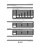
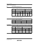
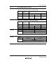
Table 8.21 Port 9 Pin Functions
Pin Selection Method and Pin Functions
P97/WAIT/SDA0 The pin function is switched as shown below according to the combination of
operating mode, bit WMS1 in WSCR, bit ICE in ICCR of IIC0, and bit P97DDR.
Operating
mode
Modes 1, 2, 3 (EXPE = 1) Modes 2, 3 (EXPE = 0)
WMS1 0 1 —
ICE 0 1 — 01
P97DDR 0 1 —— 01—
Pin function P97
input
pin
P97
output
pin
SDA0
I/O pin
WAIT
input
pin
P97
input
pin
P97
output
pin
SDA0
I/O pin
When this pin is set as the P97 output pin in the H8S/2148 Group and
H8S/2147N, it is an NMOS push-pull output. SDA0 is an NMOS open-drain
output, and has direct bus drive capability.
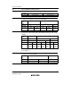
P96/φ/EXCL The pin function is switched as shown below according to the combination of
bit EXCLE in LPWRCR and bit P96DDR.
P96DDR 0 1
EXCLE 0 1 0
Pin function P96 input pin EXCL input pin φ output pin
When this pin is used as the EXCL input pin, P96DDR should be cleared to 0.
P95/AS/IOS/CS1 The pin function is switched as shown below according to the combination of
operating mode, bit IOSE in SYSCR, bit HI12E in SYSCR2, and bit P95DDR.
Operating
mode
Modes 1, 2, 3
(EXPE = 1)
Modes 2, 3 (EXPE = 0)
HI12E — 01
P95DDR — 01—
IOSE 0 1 ———
Pin function AS
output pin
IOS
output pin
P95
input pin
P95
output pin
CS1
input pin