
Datasheet

Section 11 16-Bit Free-Running Timer
Rev. 4.00 Sep 27, 2006 page 326 of 1130
REJ09B0327-0400
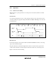
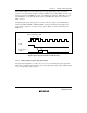
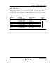
N + 1N
FRC input
clock
φ
FRC
External
clock input pin
Figure 11.4 Increment Timing with External Clock Source
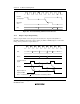
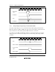
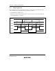
11.3.2 Output Compare Output Timing
When a compare-match occurs, the logic level selected by the output level bit (OLVLA or
OLVLB) in TOCR is output at the output compare pin (FTOA or FTOB). Figure 11.5 shows the
timing of this operation for compare-match A.
N + 1NN + 1N
N
OCRA
φ
Compare-match A
signal
FRC
OLVLA
Output compare A
output pin FTOA
Clear
*
Note: * Vertical arrows ( ) indicate instructions executed by software.
N
Figure 11.5 Timing of Output Compare A Output