
Datasheet

Section 12 8-Bit Timers
Rev. 4.00 Sep 27, 2006 page 356 of 1130
REJ09B0327-0400
12.2.6 Serial/Timer Control Register (STCR)
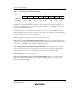
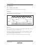
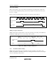
7
IICS
0
R/W
6
IICX1
0
R/W
5
IICX0
0
R/W
4
IICE
0
R/W
3
FLSHE
0
R/W
0
ICKS0
0
R/W
2
—
0
R/W
1
ICKS1
0
R/W
Bit
Initial value
Read/Write
STCR is an 8-bit readable/writable register that controls register access, the IIC operating mode
(when the on-chip IIC option is included), and on-chip flash memory (in F-ZTAT versions), and
also selects the TCNT input clock.
For details on functions not related to the 8-bit timers, see section 3.2.4, Serial Timer Control
Register (STCR), and the descriptions of the relevant modules. If a module controlled by STCR is
not used, do not write 1 to the corresponding bit.
STCR is initialized to H'00 by a reset and in hardware standby mode.
Bits 7 to 4—I
2
C Control (IICS, IICX1, IICX0, IICE): These bits control the bus buffer function
of port A and the operation of the I
2
C bus interface when the IIC option is included on-chip. See
section 16.2.7, Serial/Timer Control Register (STCR), for details.
Bit 3—Flash Memory Control Register Enable (FLSHE): Controls CPU access to the flash
memory control registers, the power-down mode control registers, and the supporting module
control registers. See section 3.2.4, Serial Timer Control Register (STCR), for details..
Bit 2—Reserved: Do not write 1 to this bit.
Bits 1 and 0—Internal Clock Select 1 and 0 (ICKS1, ICKS0): These bits, together with bits
CKS2 to CKS0 in TCR, select the clock to be input to TCNT. For details, see section 12.2.4,
Timer Control Register (TCR).