
Datasheet

Section 13 Timer Connection
Rev. 4.00 Sep 27, 2006 page 382 of 1130
REJ09B0327-0400
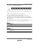
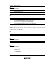
Bits 3 to 0—Input Synchronization Signal Inversion (HFINV, VFINV, HIINV, VIINV):
These bits select inversion of the input phase of the spare horizontal synchronization signal
(HFBACKI), the spare vertical synchronization signal (VFBACKI), the horizontal
synchronization signal and composite synchronization signal (HSYNCI, CSYNCI), and the
vertical synchronization signal (VSYNCI).
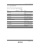
Bit 3
HFINV Description
0 The HFBACKI pin state is used directly as the HFBACKI input (Initial value)
1 The HFBACKI pin state is inverted before use as the HFBACKI input
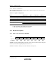
Bit 2
VFINV Description
0 The VFBACKI pin state is used directly as the VFBACKI input (Initial value)
1 The VFBACKI pin state is inverted before use as the VFBACKI input
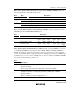
Bit 1
HIINV Description
0 The HSYNCI and CSYNCI pin states are used directly as the HSYNCI
and CSYNCI inputs (Initial value)
1 The HSYNCI and CSYNCI pin states are inverted before use as the HSYNCI and
CSYNCI inputs
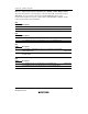
Bit 0
VIINV Description
0 The VSYNCI pin state is used directly as the VSYNCI input (Initial value)
1 The VSYNCI pin state is inverted before use as the VSYNCI input