
Datasheet


Section 14 Watchdog Timer (WDT)
Rev. 4.00 Sep 27, 2006 page 414 of 1130
REJ09B0327-0400
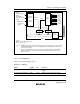
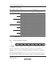
• WDT1 input clock selection
Bit 4 Bit 2 Bit 1 Bit 0 Description
PSS CKS2 CKS1 CKS0 Clock
Overflow Period
*
(when φ
φφ
φ = 20 MHz
and φ
φφ
φ
SUB
= 32.768 kHz)
0000 φ/2 (Initial value) 25.6 µs
1 φ/64 819.2 µs
10 φ/128 1.6 ms
1 φ/512 6.6 ms
100 φ/2048 26.2 ms
1 φ/8192 104.9 ms
10 φ/32768 419.4 ms
1 φ/131072 1.68 s
1000 φSUB/2 15.6 ms
1 φSUB/4 31.3 ms
10 φSUB/8 62.5 ms
1 φSUB/16 125 ms
100 φSUB/32 250 ms
1 φSUB/64 500 ms
10 φSUB/128 1 s
1 φSUB/256 2 s
Note: * The overflow period is the time from when TCNT starts counting up from H'00 until
overflow occurs.
14.2.3 System Control Register (SYSCR)
7
CS2E
0
R/W
6
IOSE
0
R/W
5
INTM1
0
R
4
INTM0
0
R/W
3
XRST
1
R
0
RAME
1
R/W
2
NMIEG
0
R/W
1
HIE
0
R/W
Bit
Initial value
Read/Write
Only bit 3 is described here. For details on functions not related to the watchdog timer, see
sections 3.2.2 and 5.2.1, System Control Register (SYSCR), and the descriptions of the relevant
modules.
Bit 3—External Reset (XRST): Indicates the reset source. When the watchdog timer is used, a
reset can be generated by watchdog timer overflow in addition to external reset input. XRST is a