
Datasheet


Section 15 Serial Communication Interface (SCI, IrDA)
Rev. 4.00 Sep 27, 2006 page 475 of 1130
REJ09B0327-0400
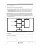
Clock
Either an internal clock generated by the built-in baud rate generator or an external serial clock
input at the SCK pin can be selected, according to the setting of the C/A bit in SMR and the CKE1
and CKE0 bits in SCR. For details on SCI clock source selection, see table 15.9.
When the SCI is operated on an internal clock, the serial clock is output from the SCK pin.
Eight serial clock pulses are output in the transfer of one character, and when no transfer is
performed the clock is fixed high. When only receive operations are performed, however, the
serial clock is output until an overrun error occurs or the RE bit is cleared to 0. To perform receive
operations in units of one character, select an external clock as the clock source.
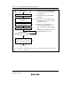
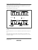
Data Transfer Operations
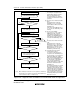
SCI Initialization (Synchronous Mode): Before transmitting and receiving data, first clear the
TE and RE bits in SCR to 0, then initialize the SCI as described below.
When the operating mode, transfer format, etc., is changed, the TE and RE bits must be cleared to
0 before making the change using the following procedure. When the TE bit is cleared to 0, the
TDRE flag is set to 1 and TSR is initialized. Note that clearing the RE bit to 0 does not change the
settings of the RDRF, PER, FER, and ORER flags, or the contents of RDR.
Figure 15.15 shows a sample SCI initialization flowchart.