
Datasheet


Section 17 Keyboard Buffer Controller
Rev. 4.00 Sep 27, 2006 page 577 of 1130
REJ09B0327-0400
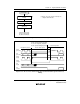
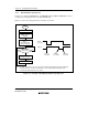
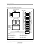
17.3.5 KCLKO and KDO Write Timing
Figure 17.10 shows the KLCKO and KDO write timing and the KCLK and KD pin states.
Internal write
signal
φ*
KCLKO, KDO
(register)
KCLK, KD
(pin state)
Note: * The φ clock shown here is scaled by 1/N in medium-speed mode when the operating
mode is active mode.
T1 T2
Figure 17.10 KCLKO and KDO Write Timing