
Datasheet


Section 20 A/D Converter
Rev. 4.00 Sep 27, 2006 page 630 of 1130
REJ09B0327-0400
20.6 Usage Notes
The following points should be noted when using the A/D converter.
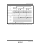
Setting Range of Analog Power Supply and Other Pins
1. Analog input voltage range
The voltage applied to the ANn analog input pins during A/D conversion should be in the
range AV
SS
≤ ANn ≤ AV
ref
(n = 0 to 7).
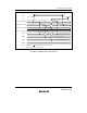
2. Digital input voltage range
The voltage applied to the CINn digital input pins should be in the range AV
SS
≤ CINn ≤ AV
ref
and V
SS
≤ CINn ≤ V
CC
(n = 0 to 15).
3. Relation between AV
CC
, AV
SS
and V
CC
, V
SS
As the relationship between AV
CC
, AV
SS
and V
CC
, V
SS
, set AV
SS
= V
SS
. If the A/D converter is
not used, the AVCC and AVSS pins must on no account be left open.
4. Setting Range of AVref Pin:
The reference voltage supplied via the AVref pin should be in the range AV
ref
≤ AV
CC
.
If conditions 1 to 4 above are not met, the reliability of the device may be adversely affected.
Notes on Board Design
In board design, digital circuitry and analog circuitry should be as mutually isolated as possible,
and layout in which digital circuit signal lines and analog circuit signal lines cross or are in close
proximity should be avoided as far as possible. Failure to do so may result in incorrect operation
of the analog circuitry due to inductance, adversely affecting A/D conversion values.
Also, digital circuitry must be isolated from the analog input signals (AN0 to AN7), analog
reference power supply (AVref), and analog power supply (AVCC) by the analog ground (AVSS).
Also, the analog ground (AVSS) should be connected at one point to a stable digital ground (VSS)
on the board.
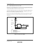
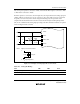
Notes on Noise Countermeasures
A protection circuit connected to prevent damage due to an abnormal voltage such as an excessive
surge at the analog input pins (AN0 to AN7) or analog reference power supply pin (AVref) should
be connected between AVCC and AVSS as shown in figure 20.7.