
Datasheet


Section 20 A/D Converter
Rev. 4.00 Sep 27, 2006 page 634 of 1130
REJ09B0327-0400
Permissible Signal Source Impedance
Analog input in this LSI is designed so that conversion precision is guaranteed for an input signal
for which the signal source impedance is 10 kΩ (AVcc = 4.0 to 5.5 V, when φ ≤ 12 MHz) or less.
This specification is provided to enable the A/D converter’s sample-and-hold circuit input
capacitance to be charged within the sampling time; if the sensor output impedance exceeds 10 kΩ
(AVcc = 4.0 to 5.5 V, when φ ≤ 12 MHz), charging may be insufficient and it may not be possible
to guarantee the A/D conversion precision.
However, if a large capacitance is provided externally, the input load will essentially comprise
only the internal input resistance of 10 kΩ, and the signal source impedance is ignored.
But since a low-pass filter effect is obtained in this case, it may not be possible to follow an analog
signal with a large differential coefficient (e.g., 5 mV/µsec or greater).
When converting a high-speed analog signal, a low-impedance buffer should be inserted.
Influences on Absolute Precision
Adding capacitance results in coupling with GND, and therefore noise in GND may adversely
affect absolute precision. Be sure to make the connection to an electrically stable GND such as
AV
SS
.
Care is also required to insure that filter circuits do not communicate with digital signals on the
mounting board, so acting as antennas.
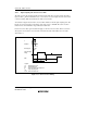
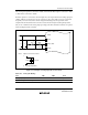
A/D converter
equivalent circuit
This LSI
20 pF
C
in
=
15 pF
10 kΩ
Low-pass
filter
C to 0.1 µF
Sensor output
impedance,
up to 10 kΩ
Sensor input
Note: Values are reference values.
Figure 20.11 Example of Analog Input Circuit