
Datasheet


Section 22 ROM (Mask ROM Version, H8S/2148 F-ZTAT, H8S/2147N F-ZTAT, H8S/2144 F-ZTAT, and H8S/2142 F-ZTAT)
Rev. 4.00 Sep 27, 2006 page 663 of 1130
REJ09B0327-0400
FLMCR1. The time during which the P bit is set is the flash memory programming time. Make a
program setting so that the time for one programming operation is within the range of (z) µs.
22.7.2 Program-Verify Mode
In program-verify mode, the data written in program mode is read to check whether it has been
correctly written in the flash memory.
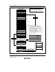
After the elapse of a given programming time, the programming mode is exited (the P bit in
FLMCR1 is cleared, then the PSU bit in FLMCR2 is cleared at least (α) µs later). The watchdog
timer is cleared after the elapse of (β) µs or more, and the operating mode is switched to program-
verify mode by setting the PV bit in FLMCR1. Before reading in program-verify mode, a dummy
write of H'FF data should be made to the addresses to be read. The dummy write should be
executed after the elapse of (γ) µs or more. When the flash memory is read in this state (verify data
is read in 16-bit units), the data at the latched address is read. Wait at least (ε) µs after the dummy
write before performing this read operation. Next, the originally written data is compared with the
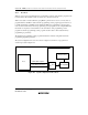
verify data, and reprogram data is computed (see figure 22.12) and transferred to the reprogram
data area. After 32 bytes of data have been verified, exit program-verify mode, wait for at least (η)
µs, then clear the SWE bit in FLMCR1. If reprogramming is necessary, set program mode again,
and repeat the program/program-verify sequence as before. However, ensure that the
program/program-verify sequence is not repeated more than (N) times on the same bits.