
Datasheet


Section 1 Overview
Rev. 4.00 Sep 27, 2006 page 28 of 1130
REJ09B0327-0400
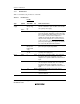
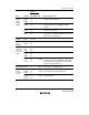
Pin No.
Type Symbol
FP-100B
TFP-100B I/O Name and Function
Bus control WAIT 16 Input Wait: Requests insertion of a wait state in the bus
cycle when accessing external 3-state address
space.
RD 22 Output Read: When this pin is low, it indicates that the
external address space is being read.
HWR 19 Output High write: When this pin is low, it indicates that
the external address space is being written to. The
upper half of the data bus is valid.
LWR 25 Output Low write: When this pin is low, it indicates that the
external address space is being written to. The
lower half of the data bus is valid.
AS/IOS 18 Output Address strobe: When this pin is low, it indicates
that address output on the address bus is valid.
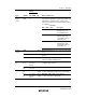
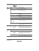
Interrupt
signals
NMI 7 Input Nonmaskable interrupt: Requests a nonmaskable
interrupt.
IRQ0 to
IRQ7
23 to 25,
97 to 99,
34, 35
Input Interrupt request 0 to 7: These pins request a
maskable interrupt.
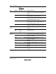
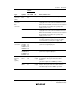
FTCI 26 Input FRT counter clock input: Input pin for an external
clock signal for the free-running counter (FRC).
16-bit free-
running
timer (FRT)
FTOA 27 Output FRT output compare A output: The output
compare A output pin.
FTOB 34 Output FRT output compare B output: The output
compare B output pin.
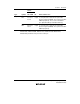
FTIA 28 Input FRT input capture A input: The input capture A
input pin.
FTIB 29 Input FRT input capture B input: The input capture B
input pin.
FTIC 32 Input FRT input capture C input: The input capture C
input pin.
FTID 33 Input FRT input capture D input: The input capture D
input pin.