
Datasheet

Section 23 ROM (H8S/2148 F-ZTAT A-Mask Version, H8S/2147 F-ZTAT A-Mask Version, H8S/2144 F-ZTAT A-Mask Version)
Rev. 4.00 Sep 27, 2006 page 695 of 1130
REJ09B0327-0400
23.5 Register Descriptions
23.5.1 Flash Memory Control Register 1 (FLMCR1)
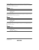
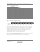
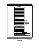
Bit 76543210
FWE SWE ——EV PV E P
Initial value10000000
Read/Write R R/W ——R/W R/W R/W R/W
FLMCR1 is an 8-bit register used for flash memory operating mode control. Program-verify mode
or erase-verify mode is entered by setting SWE to 1. Program mode is entered by setting SWE to
1, then setting the PSU bit in FLMCR2, and finally setting the P bit. Erase mode is entered by
setting SWE to 1, then setting the ESU bit in FLMCR2, and finally setting the E bit. FLMCR1 is
initialized to H'80 by a reset, and in hardware standby mode, software standby mode, subactive
mode, subsleep mode, and watch mode. When on-chip flash memory is disabled, a read will return
H'00, and writes are invalid.
Writes to the EV and PV bits in FLMCR1 are enabled only when SWE=1; writes to the E bit only
when SWE = 1, and ESU = 1; and writes to the P bit only when SWE = 1, and PSU = 1.
Bit 7—Flash Write Enable (FWE): Sets hardware protection against flash memory
programming/erasing. This bit cannot be modified and is always read as 1.
Bit 6—Software Write Enable (SWE): Enables or disables flash memory programming. SWE
should be set before setting bits ESU, PSU, EV, PV, E, P, and EB9 to EB0, and should not be
cleared at the same time as these bits.
Bit 6
SWE Description
0 Writes disabled (Initial value)
1 Writes enabled
Bit 5 and 4—Reserved: These bits cannot be modified and are always read as 0.