
Datasheet

Section 23 ROM (H8S/2148 F-ZTAT A-Mask Version, H8S/2147 F-ZTAT A-Mask Version, H8S/2144 F-ZTAT A-Mask Version)
Rev. 4.00 Sep 27, 2006 page 708 of 1130
REJ09B0327-0400
23.7 Programming/Erasing Flash Memory
In the on-board programming modes, flash memory programming and erasing is performed by
software, using the CPU. There are four flash memory operating modes: program mode, erase
mode, program-verify mode, and erase-verify mode. Transitions to these modes can be made by
setting the PSU and ESU bits in FLMCR2, and the P, E, PV, and EV bits in FLMCR1.
The flash memory cannot be read while being programmed or erased. Therefore, the program that
controls flash memory programming/erasing (the programming control program) should be
located and executed in on-chip RAM or external memory.
Notes: 1. Operation is not guaranteed if setting/resetting of the SWE, EV, PV, E, and P bits in
FLMCR1, and the ESU and PSU bits in FLMCR2, is executed by a program in flash
memory.
2. Perform programming in the erased state. Do not perform additional programming on
previously programmed addresses.
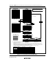
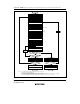
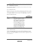
23.7.1 Program Mode
Follow the procedure shown in the program/program-verify flowchart in figure 23.12 to write data
or programs to flash memory. Performing program operations according to this flowchart will
enable data or programs to be written to flash memory without subjecting the device to voltage
stress or sacrificing program data reliability. Programming should be carried out 128 bytes at a
time.
The wait times (x, y, z1, z2, z3, α, ß, γ, ε, η, θ) after setting/clearing individual bits in flash
memory control registers 1 and 2 (FLMCR1, FLMCR2) and the maximum number of writes (N),
see section 26.2.6, Flash Memory Characteristics.
Following the elapse of (x) µs or more after the SWE bit is set to 1 in flash memory control
register 1 (FLMCR1), 128-byte program data is stored in the program data area and reprogram
data area, and the 128-byte data in the reprogram data area written consecutively to the write
addresses. The lower 8 bits of the first address written to must be H'00 or H'80. 128 consecutive
byte data transfers are performed. The program address and program data are latched in the flash
memory. A 128-byte data transfer must be performed even if writing fewer than 128 bytes; in this
case, H'FF data must be written to the extra addresses.
Next, the watchdog timer is set to prevent overprogramming in the event of program runaway, etc.
Set a value greater than (y + z2 + α + β) µs as the WDT overflow period. After this, preparation
for program mode (program setup) is carried out by setting the PSU bit in FLMCR2, and after the
elapse of (y) µs or more, the operating mode is switched to program mode by setting the P bit in
FLMCR1. The time during which the P bit is set is the flash memory programming time. Make a