
Datasheet

Section 25 Power-Down State
Rev. 4.00 Sep 27, 2006 page 751 of 1130
REJ09B0327-0400
Bit 5
NESEL Description
0 Sampling at φ divided by 32 (Initial value)
1 Sampling at φ divided by 4
Bit 4—Subclock Input Enable (EXCLE): Controls subclock input from the EXCL pin.
Bit 4
EXCLE Description
0 Subclock input from EXCL pin is disabled (Initial value)
1 Subclock input from EXCL pin is enabled
Bits 3 to 0—Reserved: These bits cannot be modified and are always read as 0.
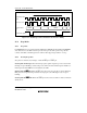
25.2.3 Timer Control/Status Register (TCSR)
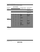
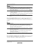
TCSR1
7
OVF
0
R/(W)
*
6
WT/IT
0
R/W
5
TME
0
R/W
4
PSS
0
R/W
3
RST/NMI
0
R/W
0
CKS0
0
R/W
2
CKS2
0
R/W
1
CKS1
0
R/W
Bit
Initial value
Read/Write
Note: * Only 0 can be written in bit 7, to clear the flag.
TCSR1 is an 8-bit readable/writable register that performs selection of the WDT1 TCNT input
clock, mode, etc.
Only bit 4 is described here. For details of the other bits, see section 14.2.2, Timer Control/Status
Register (TCSR).
TCSR is initialized to H'00 by a reset and in hardware standby mode. It is not initialized in
software standby mode.
Bit 4—Prescaler Select (PSS): Selects the WDT1 TCNT input clock.
This bit also controls the operation in a power-down mode transition. The operating mode to
which a transition is made after execution of a SLEEP instruction is determined in combination
with other control bits.