
Datasheet

Section 26 Electrical Characteristics
Rev. 4.00 Sep 27, 2006 page 784 of 1130
REJ09B0327-0400
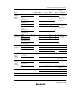
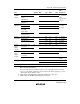
Table 26.5 Bus Drive Characteristics
Conditions: V
CC
= 3.0 V to 5.5 V, V
SS
= 0 V
Applicable Pins: SCL1, SCL0, SDA1, SDA0 (bus drive function selected)
Item Symbol Min Typ Max Unit Test Conditions
V
T
–
V
CC
× 0.3 —— VV
CC
= 3.0 V to 5.5 VSchmitt trigger
input voltage
V
T
+
——V
CC
× 0.7 V
CC
= 3.0 V to 5.5 V
V
T
+
– V
T
–
V
CC
× 0.05 —— V
CC
= 3.0 V to 5.5 V
Input high voltage V
IH
V
CC
× 0.7 — V
CC
+0.5 V V
CC
= 3.0 V to 5.5 V
Input low voltage V
IL
–0.5 — V
CC
× 0.3 V
CC
= 3.0 V to 5.5 V
Output low voltage V
OL
——0.8 V I
OL
= 16 mA,
V
CC
= 4.5 V to 5.5 V
——0.5 I
OL
= 8 mA
——0.4 I
OL
= 3 mA
Input capacitance C
in
——20 pF V
in
= 0 V, f = 1 MHz,
T
a
= 25°C
Three-state leakage
current (off state)
| I
TSI
| ——1.0 µA V
in
= 0.5 to V
CC
–0.5 V
SCL, SDA output
fall time
t
Of
20 + 0.1 Cb — 250 ns V
CC
= 3.0 V to 5.5 V
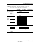
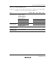
Conditions: V
CC
= 3.0 V to 5.5 V, V
CC
B = 3.0 V to 5.5 V, V
SS
= 0 V
Applicable Pins: PS2AC, PS2AD, PS2BC, PS2BD, PS2CC, PS2CD, PA7 to PA4 (bus drive
function selected)
Item Symbol Min Typ Max Unit Test Conditions
Output low voltage V
OL
——0.8 V I
OL
= 16 mA,
V
CC
B = 4.5 V to 5.5 V
——0.5 I
OL
= 8 mA
——0.4 I
OL
= 3 mA
26.2.3 AC Characteristics
Clock timing, control signal timing, bus timing, and timing of on-chip supporting modules list the
following.
Figure 26.4 shows the test conditions for the AC characteristics.