
Datasheet


Section 26 Electrical Characteristics
Rev. 4.00 Sep 27, 2006 page 795 of 1130
REJ09B0327-0400
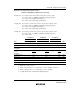
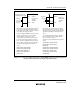
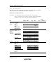
Table 26.11 I
2
C Bus Timing
Conditions: V
CC
= 3.0 V to 5.5 V, V
SS
= 0 V, φ = 5 MHz to maximum operating frequency
Ratings
Item Symbol Min Typ Max Unit Test Conditions Notes
SCL input cycle
time
t
SCL
12 ——t
cyc
Figure 26.28
SCL input high
pulse width
t
SCLH
3 ——t
cyc
SCL input low
pulse width
t
SCLL
5 ——t
cyc
SCL, SDA input
rise time
t
Sr
——7.5
*
t
cyc
SCL, SDA input
fall time
t
Sf
——300 ns
SCL, SDA input
spike pulse
elimination time
t
SP
——1t
cyc
SDA input bus
free time
t
BUF
5 ——t
cyc
Start condition
input hold time
t
STAH
3 ——t
cyc
Retransmission
start condition
input setup time
t
STAS
3 ——t
cyc
Stop condition
input setup time
t
STOS
3 ——t
cyc
Data input setup
time
t
SDAS
0.5 ——t
cyc
Data input hold
time
t
SDAH
0 ——ns
SCL, SDA
capacitive load
C
b
——400 pF
Note: * 17.5t
cyc
can be set according to the clock selected for use by the I
2
C module. For details,
see section 16.4, Usage Notes.