
Datasheet

Section 26 Electrical Characteristics
Rev. 4.00 Sep 27, 2006 page 836 of 1130
REJ09B0327-0400
26.4 Electrical Characteristics of H8S/2147N F-ZTAT
26.4.1 Absolute Maximum Ratings
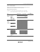
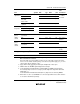
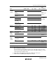
Table 26.30 lists the absolute maximum ratings.
Table 26.30 Absolute Maximum Ratings
Item Symbol Value Unit
Power supply voltage
*
V
CC
–0.3 to +7.0 V
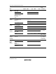
Input/output buffer power supply
(power supply for the port A)
V
CC
B –0.3 to +7.0 V
Input voltage (except ports 6, 7,
and A)
V
in
–0.3 to V
CC
+0.3 V
Input voltage (CIN input not
selected for port 6)
V
in
–0.3 to V
CC
+0.3 V
Input voltage (CIN input not
selected for port A)
V
in
–0.3 to V
CC
B +0.3 V
Input voltage (CIN input selected
for port 6)
V
in
–0.3 V to lower of voltages V
CC
+0.3 and
AV
CC
+0.3
V
Input voltage (CIN input selected
for port A)
V
in
–0.3 V to lower of voltages V
CC
B +0.3 and
AV
CC
+0.3
V
Input voltage (port 7) V
in
–0.3 to AV
CC
+0.3 V
Reference supply voltage AV
ref
–0.3 to AV
CC
+0.3 V
Analog power supply voltage AV
CC
–0.3 to +7.0 V
Analog input voltage V
AN
–0.3 to AV
CC
+0.3 V
Operating temperature T
opr
Regular specifications: –20 to +75 °C
Operating temperature (flash
memory programming/erasing)
T
opr
Regular specifications: 0 to +75 °C
Storage temperature T
stg
–55 to +125 °C
Caution: Permanent damage to the chip may result if absolute maximum ratings are exceeded.
Note: * Power supply voltage for VCC1 and VCC2 pins.