
Datasheet


Section 26 Electrical Characteristics
Rev. 4.00 Sep 27, 2006 page 848 of 1130
REJ09B0327-0400
(1) Clock Timing
Table 26.34 shows the clock timing. The clock timing specified here covers clock (φ) output and
clock pulse generator (crystal) and external clock input (EXTAL pin) oscillation settling times.
For details of external clock input (EXTAL pin and EXCL pin) timing, see section 24, Clock
Pulse Generator.
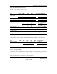
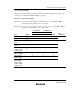
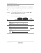
Table 26.34 Clock Timing
Condition A: V
CC
= 5.0 V ±10%, V
CC
B = 5.0 V ±10%, V
SS
= 0 V, φ = 2 MHz to maximum
operating frequency, T
a
= –20 to +75°C
Condition B: V
CC
= 3.0 V to 5.5 V, V
CC
B = 3.0 V to 5.5 V, V
SS
= 0 V, φ = 2 MHz to maximum
operating frequency, T
a
= –20 to +75°C
Condition A Condition B
20 MHz 10 MHz
Item Symbol Min Max Min Max Unit
Test
Conditions
Clock cycle time t
cyc
50 500 100 500 ns Figure 26.5
Clock high pulse
width
t
CH
17 — 30 — ns Figure 26.5
Clock low pulse
width
t
CL
17 — 30 — ns
Clock rise time t
Cr
—8 —20 ns
Clock fall time t
Cf
—8 —20 ns
Oscillation settling
time at reset
(crystal)
t
OSC1
10 — 20 — ms Figure 26.6
Figure 26.7
Oscillation settling
time in software
standby (crystal)
t
OSC2
8— 8— ms
External clock
output stabilization
delay time
t
DEXT
500 — 500 — µs