
Datasheet

Section 26 Electrical Characteristics
Rev. 4.00 Sep 27, 2006 page 880 of 1130
REJ09B0327-0400
(4) Timing of On-Chip Supporting Modules
Tables 26.51 shows the on-chip supporting module timing. The only on-chip supporting modules
that can operate in subclock operation (φ = 32.768 kHz) are the I/O ports, external interrupts (NMI
and IRQ0, 1, 2, 6, and 7), the watchdog timer, and the 8-bit timer (channels 0 and 1).
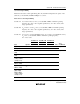
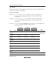
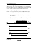
Table 26.51 Timing of On-Chip Supporting Modules
Condition A: V
CC
= 5.0 V ±10%, V
SS
= 0 V, φ = 32.768 kHz
*
, 2 MHz to maximum operating
frequency, T
a
= –20 to +75°C (regular specifications), T
a
= –40 to +85°C (wide-
range specifications)
Condition B: V
CC
= 4.0 V to 5.5 V, V
SS
= 0 V, φ = 32.768 kHz
*
, 2 MHz to maximum operating
frequency, T
a
= –20 to +75°C (regular specifications), T
a
= –40 to +85°C (wide-
range specifications)
Condition C: V
CC
= 2.7 V to 5.5 V (mask ROM version), V
CC
= 3.0 V to 5.5 V (F-ZTAT version),
V
SS
= 0 V, φ = 32.768 kHz
*
, 2 MHz to maximum operating frequency,
T
a
= –20 to +75°C
Condition A Condition B Condition C
20 MHz 16 MHz 10 MHz
Item Symbol Min Max Min Max Min Max Unit
Test
Conditions
I/O
ports
Output data delay
time
t
PWD
— 50 — 50 — 100 ns Figure
26.15
Input data setup
time
t
PRS
30 — 30 — 50 —
Input data hold
time
t
PRH
30 — 30 — 50 —
FRT
Timer output
delay
time
t
FTOD
— 50 — 50 — 100
ns Figure
26.16
Timer input setup
time
t
FTIS
30 — 30 — 50 —
Timer clock input
setup time
t
FTCS
30 — 30 — 50 — Figure
26.17
Single
edge
t
FTCWH
1.5 — 1.5 — 1.5 — t
cyc
Timer
clock
pulse
width
Both
edges
t
FTCWL
2.5 — 2.5 — 2.5 —