
Datasheet


Section 26 Electrical Characteristics
Rev. 4.00 Sep 27, 2006 page 897 of 1130
REJ09B0327-0400
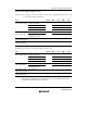
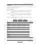
Table 26.58 Permissible Output Currents
Conditions: V
CC
= 4.0 V to 5.5 V, V
SS
= 0 V, Ta = –20 to +75°C (regular specifications), T
a
= –40
to +85°C (wide-range specifications)
Item Symbol Min Typ Max Unit
Permissible output
low current (per pin)
PA7 to PA4 (bus drive
function selected)
I
OL
——20mA
Ports 1, 2, 3 — — 10 mA
RESO ——3 mA
Other output pins — — 2 mA
Total of ports 1, 2, and 3 ∑ I
OL
——80mAPermissible output
low current (total)
Total of all output pins,
including the above
— — 120 mA
Permissible output
high current (per pin)
All output pins –I
OH
——2 mA
Permissible output
high current (total)
Total of all output pins ∑ –I
OH
——40mA
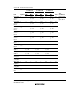
Conditions: V
CC
= 2.7 V to 3.6 V, V
SS
= 0 V, T
a
= –20 to +75°C
Item Symbol Min Typ Max Unit
Permissible output
low current (per pin)
PA7 to PA4 (bus drive
function selected)
I
OL
——10mA
Ports 1, 2, 3 — — 2 mA
RESO ——1 mA
Other output pins — — 1 mA
Total of ports 1, 2, and 3 ∑ I
OL
——40mAPermissible output
low current (total)
Total of all output pins,
including the above
——60mA
Permissible output
high current (per pin)
All output pins –I
OH
——2 mA
Permissible output
high current (total)
Total of all output pins ∑ –I
OH
——30mA
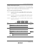
Notes: 1. To protect chip reliability, do not exceed the output current values in table 26.58.
2. When driving a Darlington pair or LED, always insert a current-limiting resistor in the
output line, as show in figures 26.1 and 26.2.