
Datasheet

Section 26 Electrical Characteristics
Rev. 4.00 Sep 27, 2006 page 905 of 1130
REJ09B0327-0400
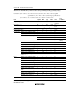
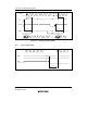
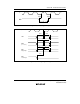
26.6.4 A/D Conversion Characteristics
Tables 26.64 and 26.65 list the A/D conversion characteristics.
Table 26.64 A/D Conversion Characteristics
(AN7 to AN0 Input: 134/266-State Conversion)
Condition A: V
CC
= 5.0 V ±10%, AV
CC
= 5.0 V ±10%, AV
ref
= 4.5 V to AV
CC
,
V
SS
= AV
SS
= 0 V, φ = 2 MHz to maximum operating frequency,
T
a
= –20 to +75°C (regular specifications),
T
a
= –40 to +85°C (wide-range specifications)
Condition B: V
CC
= 4.0 V to 5.5 V, AV
CC
= 4.0 V to 5.5 V, AV
ref
= 4.0 V to AV
CC
,
V
SS
= AV
SS
= 0 V, φ = 2 MHz to maximum operating frequency,
T
a
= –20 to +75°C (regular specifications),
T
a
= –40 to +85°C (wide-range specifications)
Condition C: V
CC
= 2.7 V to 3.6 V, AV
CC
= 2.7 V to 3.6 V, AV
ref
= 2.7 V to AV
CC
,
V
SS
= AV
SS
= 0 V, φ = 2 MHz to maximum operating frequency,
T
a
= –20 to +75°C
Condition A Condition B Condition C
20 MHz 16 MHz 10 MHz
Item Min Typ Max Min Typ Max Min Typ Max Unit
Resolution 10 10 10 10 10 10 10 10 10 Bits
Conversion time
*
3
——6.7 ——8.4 ——13.4µs
Analog input
capacitance
——20 ——20 ——20 pF
——10
*
1
——10
*
1
——5 kΩPermissible signal-
source impedance
5
*
2
5
*
2
Nonlinearity error — — ±3.0 — — ±3.0 — — ±7.0 LSB
Offset error ——±3.5——±3.5——±7.5LSB
Full-scale error — — ±3.5 — — ±3.5 — — ±7.5 LSB
Quantization error — — ±0.5 — — ±0.5 — — ±0.5 LSB
Absolute accuracy——±4.0——±4.0——±8.0LSB
Notes: 1. When conversion time ≥ 11. 17 µs (CKS = 1 and φ ≤ 12 MHz, or CKS = 0)
2. When conversion time < 11. 17 µs (CKS = 1 and φ > 12 MHz)
3. In single mode and φ = maximum operating frequency.