
Datasheet

Section 8 I/O Ports
Rev.7.00 Dec. 24, 2008 Page 219 of 698
REJ09B0074-0700
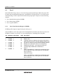
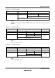
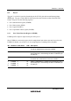
Table 8.6 P14 Pin Function
TPU Channel 1 Setting*
1
Output Setting Input Setting or Initial Value
P14DDR ⎯ 0 1
P14 input pin P14 output pin TIOCA1 output pin
TIOCA1 input pin
Pin Function
IRQ0 input pin*
2
Notes: 1. For details on the TPU channel setting, refer to section 9, 16-Bit Timer Pulse Unit
(TPU).
2. When this pin is used as an external interrupt pin, this pin must not be used for another
function.
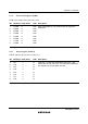
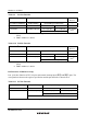
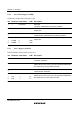
Table 8.7 P13 Pin Function
AE3 to AE0*
2
Other than B'1111 B'1111
TPU Channel 0 Setting*
1
Output Setting Input Setting or Initial Value ⎯
P13DDR ⎯ 0 1 ⎯
P13 input pin P13 output pin TIOCD0 output pin
TIOCD0 input pin
Pin Function
TCLKB input pin
A23 output
pin*
2
Notes: 1. For details on the TPU channel setting, refer to section 9, 16-Bit Timer Pulse Unit
(TPU).
2. Valid in modes 4, 5, and 6.
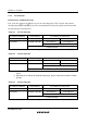
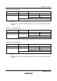
Table 8.8 P12 Pin Function
AE3 to AE0*
2
Other than B'1111 B'1111
TPU Channel 0 Setting*
1
Output Setting Input Setting or Initial Value ⎯
P12DDR ⎯ 0 1 ⎯
P12 input pin P12 output pin TIOCC0 output pin
TIOCC0 input pin
Pin Function
TCLKA input pin
A22 output
pin*
2
Notes: 1. For details on the TPU channel setting, refer to section 9, 16-Bit Timer Pulse Unit
(TPU).
2. Valid in modes 4, 5, and 6.