
Datasheet


Section 9 16-Bit Timer Pulse Unit (TPU)
Rev.7.00 Dec. 24, 2008 Page 337 of 698
REJ09B0074-0700
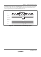
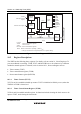
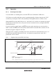
Contention between TCNT Write and Overflow/Underflow: If there is an up-count or down-
count in the T
2
state of a TCNT write cycle, and overflow/underflow occurs, the TCNT write takes
precedence and the TCFV/TCFU flag in TSR is not set. Figure 9.53 shows the operation timing
when there is contention between TCNT write and overflow.
Write signal
A
ddress
φ
TCNT address
TCNT
TCNT write cycle
T
1
T
2
H'FFFF M
TCNT write data
TCFV flag
Prohibited
Figure 9.53 Contention between TCNT Write and Overflow
Multiplexing of I/O Pins: In this LSI, the TCLKA input pin is multiplexed with the TIOCC0 I/O
pin, the TCLKB input pin with the TIOCD0 I/O pin, the TCLKC input pin with the TIOCB1 I/O
pin, and the TCLKD input pin with the TIOCB2 I/O pin. When an external clock is input, compare
match output should not be performed from a multiplexed pin.
Interrupts in Module Stop Mode: If module stop mode is entered when an interrupt has been
requested, it will not be possible to clear the CPU interrupt source or the DMAC activation source.
Interrupts should therefore be disabled before entering module stop mode.
Module Stop Mode Setting: TPU operation can be disabled or enabled using the module stop
control register. The initial setting is for TPU operation to be halted. Register access is enabled by
clearing module stop mode. For details, refer to section 20, Power-Down Modes.