
Datasheet

Section 12 Serial Communication Interface
Rev.7.00 Dec. 24, 2008 Page 384 of 698
REJ09B0074-0700
12.3.9 Serial Extended Mode Register A_0 (SEMRA_0)
SEMRA_0 extends the functions of SCI_0. SEMR0 enables selection of the SCI_0 select function
in synchronous mode, base clock setting in asynchronous mode, and also clock source selection
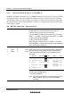
and automatic transfer rate setting. Figure 12.3 shows an example of the internal base clock when
an average transfer rate is selected and figure 12.4 shows as example of the setting when the TPU
clock input is selected.
Bit Bit Name Initial Value R/W Description
7 SSE 0 R/W SCI_0 Select Enable
Allows selection of the SCI0 select function when an
external clock is input in synchronous mode.
The SSE setting is valid when external clock input is used
(CKE1 = 1 in SCR) in synchronous mode (C/A = 1 in SMR).
0: SCI_0 select function disabled
1: SCI_0 select function enabled
When the SCI_0 select function is enabled, if 1 is input to
the PG1/IRQ7 pin, TxD0 output goes to the high-impedance
state, SCK0 input is fixed high.
6
5
4
TCS2
TCS1
TCS0
0
0
0
R/W
R/W
R/W
TPU Clock Select
When the TPU clock is input (ACS3 to ACS0 = B'0100) as
the clock source in asynchronous mode, serial transfer
clock is generated depending on the combination of the
TPU clock.
Base Clock Clock Enable TCLKA TCLKB TCLKC
000 TIOCA1 TIOCA2 Base clock written
in the left column
Pin input Pin input
001 TIOCA0 | TIOCC0 TIOCA1 Pin input Base clock written
in the left column
Pin input
010 TIOCA0 TIOCA1 & TIOCA2 Pin input Base clock written
in the left column
Pin input
011 TIOCA0 | TIOCC0 TIOCA1 & TIOCA2 Pin input Base clock written
in the left column
Pin input
1×× Reserved (Setting prohibited)
Legend:
&: AND (logical multiplication)
I : OR (logical addition)
Note: The functions of bits 6 to 4 are not supported by the
E6000 emulator. Figure 12.4 shows the setting
examples.